
About Us
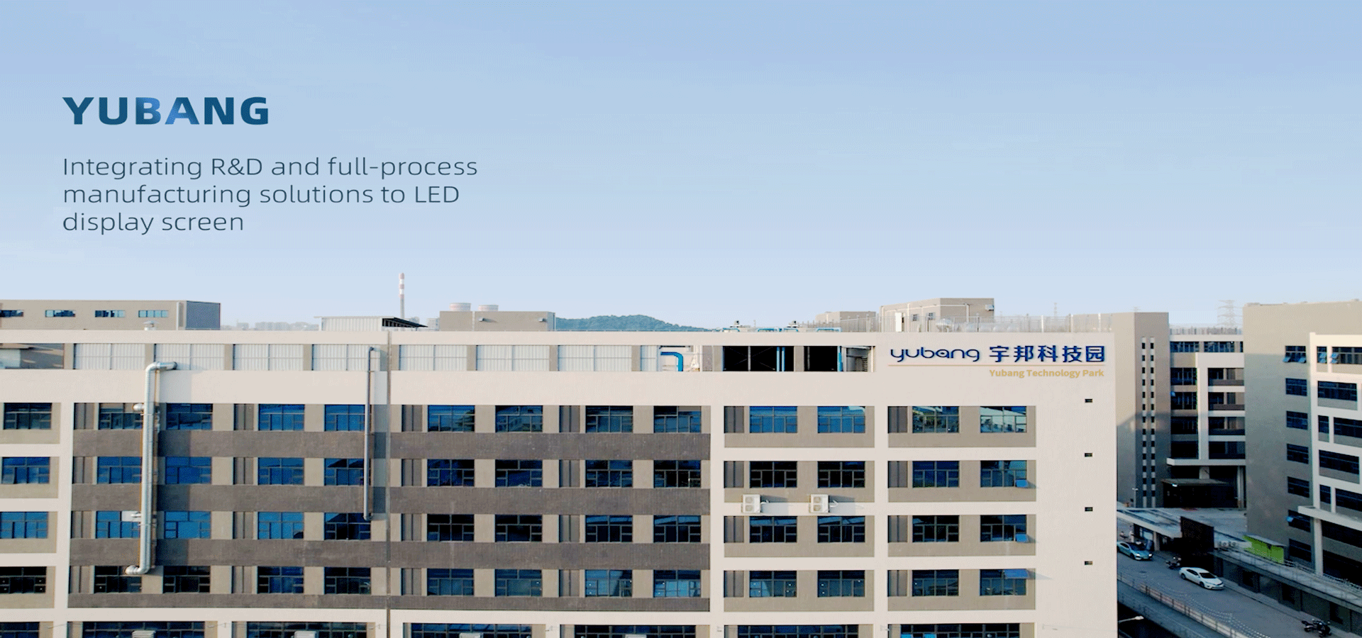
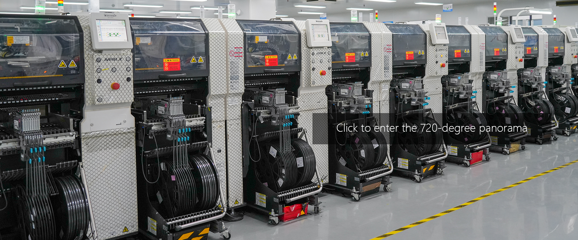
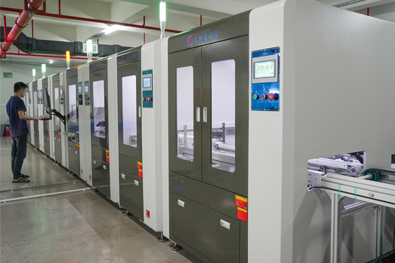
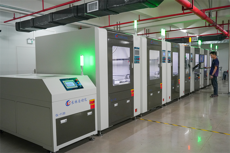
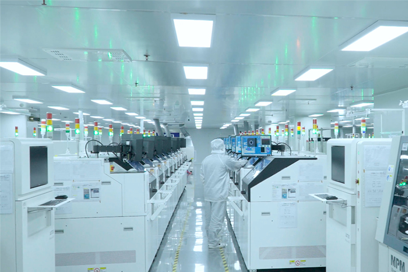
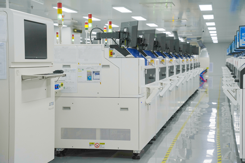
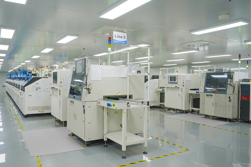
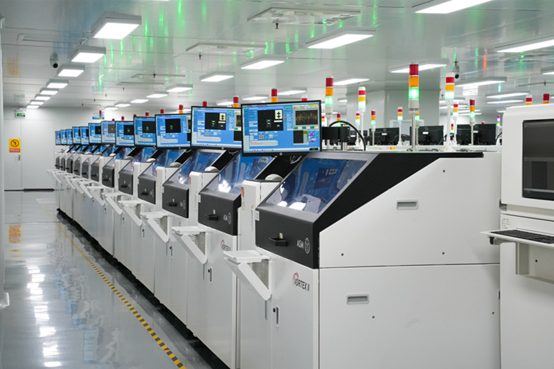
With innovation and development driven by science and technology, Shenzhen Yubang Electronics Co., Ltd. has been delving into development and manufacturing of electronic products. And Yubang Intelligent Manufacturing Industrial Park was completed and put into operation in October 2022 with a floor area of 24,000 square meters and workshop area of 60,000 square meters. Therefore, two manufacturing bases are built up in Shenzhen and Zhongshan respectively.
Introduction Video20 +
Development
6000 +
Workshop Area
20 +
Model Patents
Products
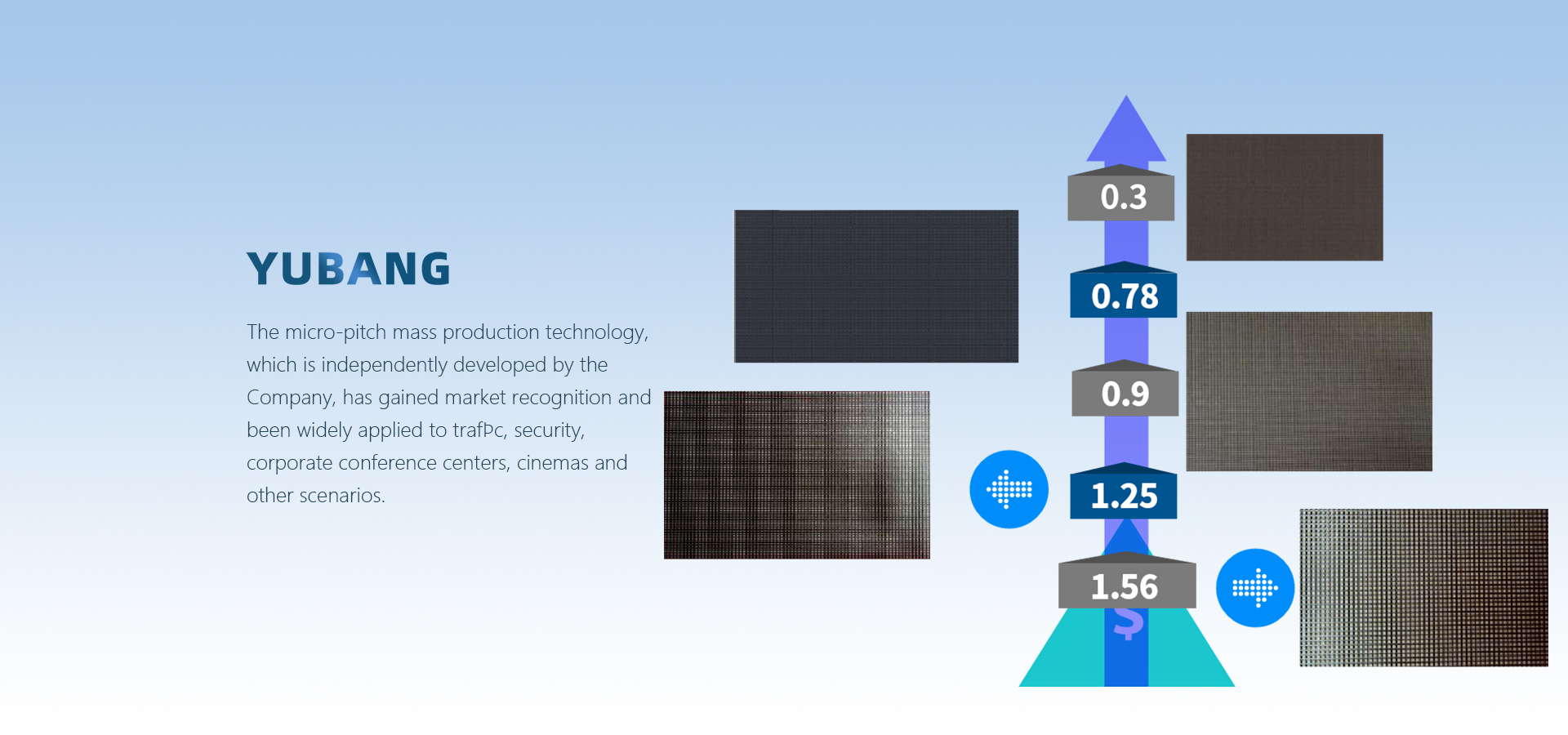
MIP
MIP
As a new Micro package technology, the MIP (Micro LED in Package) technology, coupled with self-developed ink packaging process, has such advantages as ultra-high contrast, ink color consistency, high reliability, excellent surface light source, absence of glare, ultra energy-saving cold screen, mixable light source chip, high uniformity, absence of Mura effect, and highly delicate image quality.
View DetailsCOB
COB
With ultra-small dot pitch and self-developed ink packaging process, the COB (Chip on board) technology has such advantages as ultra-high contrast, ink color consistency, high reliability, excellent surface light source, absence of glare, energy-saving cold screen and chip scale packaging, which provides a better display effect and perfect close-up experience.
View DetailsGOB
GOB
For the GOB (Glue on board) technology, an optical heat-conducting nano-filler is used to encapsulate the panel of the LED by providing it with a matte finish. In this way, a matte effect is achieved on the surface of the LED screen, and the protection capability of the LED screen is enhanced.
View DetailsPCBA
PCBA
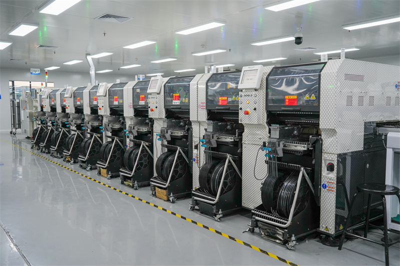
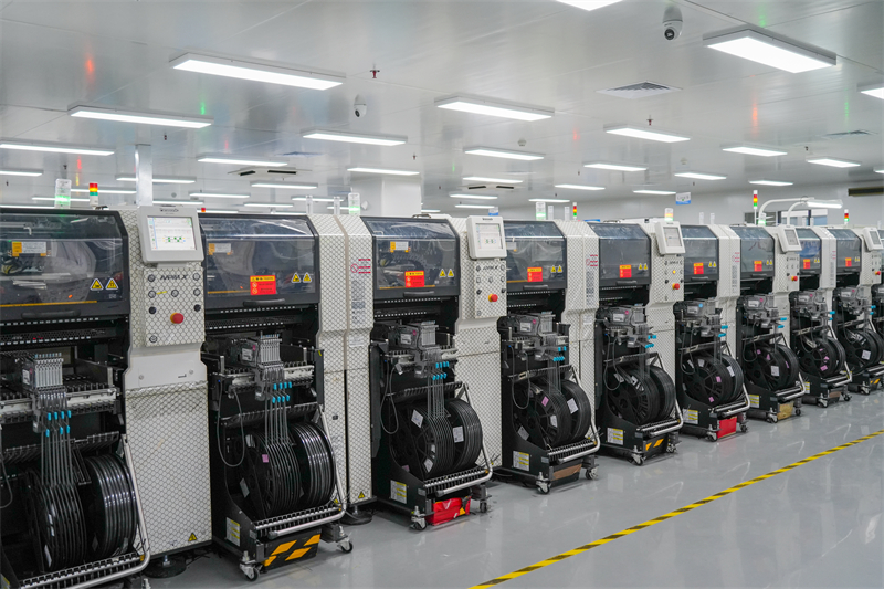
PCBA electronic product processing involves a series of production supply chains such as design document inspection, component procurement, PCB board production, SMT patching, plug-in processing, PCBA testing, packaging, etc., so it requires professional suppliers to manage it.
View DetailsNews & Video










 Download Introduction


